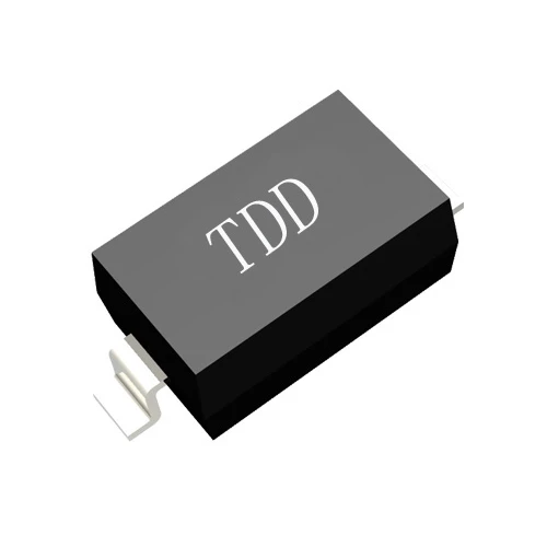
This guide to Choosing Switching Diodes for Logic-Level Signal Circuits explains how to check logic margins, leakage, capacitance, speed, and reliability, with a practical validation workflow from Shenzhen Daya Electronics Co., Ltd.
Home-Resource-Blog-Choosing Switching Diodes for Logic-Level Signal Circuits
Choosing Switching Diodes for Logic-Level Signal Circuits
Oct.27,2026
Share:
Choosing Switching Diodes for Logic-Level Signal Circuits starts with defining the signal’s voltage, current, speed, and protection needs, then comparing diode characteristics against the logic device’s guaranteed thresholds. We recommend a five-stage process: map the circuit and operating conditions, shortlist a Small Signal Switching Diode by its datasheet limits, calculate loading and timing effects, verify the design across temperature and supply extremes, and document component qualification. Whether you are new to circuit design or refining a production board, this approach helps avoid logic-level errors, slow edges, and reliability surprises. Shenzhen Daya Electronics Co., Ltd. can help buyers and design teams evaluate diode options against these requirements.
A switching diode should be selected for the complete signal path, not by part number alone.
Start with the signal path and its logic thresholds
Before selecting a diode, identify what it must do. A series diode, a steering diode, a clamp, and a signal-isolation diode can face very different electrical stresses. Choosing Switching Diodes for Logic-Level Signal Circuits is most reliable when the circuit function is written down before candidate parts are compared.
Record the essential operating conditions
Logic family and supply: Record the transmitter and receiver supply voltages, including permitted tolerances.
Input thresholds: Find the receiver’s guaranteed VIH and VIL limits in its datasheet. Do not assume that a nominal 3.3 V or 5 V signal automatically meets them.
Signal characteristics: Note the minimum pulse width, edge rate, frequency, duty cycle, and whether the line is push-pull, open-drain, or bidirectional.
Electrical stress: Establish peak forward current, reverse voltage, transient exposure, ambient temperature, and expected operating life.
Interconnection: Include the driver’s output resistance, PCB trace, connector, cable, pull-up or pull-down resistor, and receiver input capacitance.
These details establish the design envelope. A diode that works on a short bench connection may behave differently on a long cable or a high-impedance input because parasitic capacitance and leakage become more significant.
Compare diode parameters against the real design limits
Once the signal path is defined, compare guaranteed datasheet values rather than relying only on typical values. A Small Signal Switching Diode is often selected for compact signal steering or fast switching, but its forward drop, reverse leakage, capacitance, and recovery behavior can affect logic margin.
Parameter
Why it matters in a logic circuit
What to check
Forward voltage, VF
Reduces the voltage delivered through a series diode and affects clamp levels.
Check VF at the actual forward current and temperature, then recalculate the receiver’s high-level margin.
Reverse leakage, IR
Can shift a high-impedance node or alter a pull-up voltage, especially at elevated temperature.
Use the maximum specified leakage at the relevant reverse voltage and temperature.
Junction capacitance, CJ
Combines with source resistance to slow edges and distort short pulses.
Check the measurement conditions in the datasheet and include PCB and receiver capacitance.
Reverse recovery time, trr
Can affect switching behavior when the diode changes from forward conduction to reverse bias.
Compare the specified test conditions with the actual switching current and waveform.
Reverse voltage, VR
Excess reverse bias can cause leakage growth or device failure.
Allow margin for supply tolerance, ringing, and transient events.
Forward current and power
Determine whether the junction and package remain within their safe operating limits.
Check pulse and continuous ratings, derating curves, thermal resistance, and PCB heat paths.
Choose the diode type for the job
Silicon switching diode: Often appropriate for general-purpose signal steering when its forward drop and capacitance fit the logic budget.
Schottky diode: Can provide a lower forward voltage for clamping, but reverse leakage may be higher. Check the maximum leakage at the circuit’s hottest operating condition.
Low-capacitance signal diode: Worth considering for fast edges or high-impedance nodes, provided its current and voltage ratings remain adequate.
There is no universally best diode. For Choosing Switching Diodes for Logic-Level Signal Circuits, the correct choice is the part that satisfies all worst-case electrical and thermal limits while preserving adequate logic margin.
Calculate voltage margin, loading, and edge timing
Next, calculate the circuit rather than judging it by a schematic symbol. For a series diode, estimate the receiver voltage using the driver’s guaranteed output voltage, the diode’s forward drop at the relevant current, and any voltage loss in the interconnect. Then compare that result with the receiver’s guaranteed VIH requirement.
Illustrative check: If a 3.3 V driver must deliver a high level through a diode to a receiver requiring at least 2.0 V, use the driver’s minimum VOH—not its nominal supply—and the diode’s maximum VF at the expected current. The remaining voltage must exceed 2.0 V with suitable margin. This example is not a substitute for the selected IC and diode datasheets.
Estimate leakage and RC delay
Leakage can matter even when the diode carries almost no intended current. For example, 1 µA of leakage through a 10 kΩ effective pull-up resistance corresponds to a 10 mV voltage shift, using V = I × R. Recalculate with the diode’s worst-case leakage and the complete node resistance.
For a first-order timing estimate, use τ = R × C. A 10 kΩ source resistance and 10 pF total node capacitance produce a 100 ns time constant. Real rise time also depends on the driver, topology, and receiver thresholds, so verify the waveform when pulse timing is critical. This check is especially important when choosing a Small Signal Switching Diode for a high-impedance or fast logic input.
Validate the circuit in staged bench and production checks
After the calculations pass, test the assembled circuit under representative conditions. A disciplined validation plan catches faults that a nominal-voltage bench test can miss.
Confirm the circuit function: Verify that the diode orientation and intended steering or clamping path match the schematic.
Measure logic levels: Record VOH and VOL at the receiver pin, then compare them with guaranteed VIH and VIL limits.
Inspect timing: Use an oscilloscope to check rise time, fall time, overshoot, ringing, pulse width, and propagation behavior.
Test corner conditions: Repeat checks at minimum and maximum supply voltage and across the intended temperature range.
Check stress and assembly: Confirm that forward current, reverse voltage, and power remain within derated ratings; inspect polarity, solder joints, and component markings.
Document results: Record the diode manufacturer, exact part number, datasheet revision, test setup, measured values, and acceptance limits.
For component qualification, review applicable semiconductor requirements such as IEC 60747-3 for signal (small-signal) diodes, where relevant to the device and procurement specification. Environmental testing should follow the applicable project requirements and test methods; do not treat a standards reference as proof that a particular component has passed a test. Request traceability and test documentation from the supplier when they are required for the application.
Learn from a practical design example
Consider an illustrative 3.3 V controller input protected by a diode network and a 10 kΩ pull-up. During the first design review, the team focused on the diode’s low forward voltage. A corner calculation then showed that maximum reverse leakage at elevated temperature could shift the high-impedance node, while the combined input and diode capacitance lengthened the edge.
The team compared alternative Small Signal Switching Diode candidates using maximum leakage, capacitance, and forward-voltage data, then measured the final board at the receiver pin. The chosen part met the project’s logic thresholds and timing limits at the tested supply and temperature corners. This is an illustrative engineering case, not a claim about a specific customer result; it demonstrates why comparing the full datasheet and validating the assembled circuit are both necessary.
Use a repeatable sourcing and review toolkit
To make Choosing Switching Diodes for Logic-Level Signal Circuits easier across prototypes and production, keep a short engineering toolkit with every design review:
Datasheet comparison sheet: Capture maximum VF, IR, CJ, trr, VR, current ratings, package, and test conditions for each candidate.
Logic-margin worksheet: Calculate worst-case VOH and VOL at the receiver using guaranteed specifications and component tolerances.
Measurement equipment: Use a calibrated digital multimeter for steady-state checks and an oscilloscope with a suitable probe for signal integrity measurements.
Qualification record: Track lot identification, incoming inspection, revision control, and any required 100% functional testing defined by the product’s control plan.
Supplier review: Ask for the current datasheet, package and marking details, traceability information, and confirmation of the exact ordering code.
Shenzhen Daya Electronics Co., Ltd. can be included in the supplier review process when evaluating Small Signal Switching Diode options. Share the circuit’s maximum and minimum voltages, signal speed, operating temperature, package preference, and qualification requirements so the candidate review is based on application needs rather than a part-number match alone.
Resolve common selection problems before release
The logic high is too low
Recheck the driver’s minimum VOH, diode VF at the real load current, and receiver VIH. If margin is inadequate, consider a different topology, a suitable lower-drop device, or removing the series diode if the protection function can be met another way.
The signal edge is unexpectedly slow
Measure total node capacitance and source resistance, including probe loading. Review diode capacitance, pull-up resistance, trace length, and receiver input capacitance. A lower-capacitance diode or a stronger driver may help, but verify that the change does not increase current or compromise protection.
The circuit works at room temperature but fails in the field
Check worst-case leakage and forward voltage over temperature, as well as supply tolerance and transient exposure. Use guaranteed maximum and minimum values where available, and test at the specified operating corners rather than extrapolating from a room-temperature measurement.
Substituted parts behave differently
Do not approve a substitute based only on package compatibility or a similar nominal rating. Compare all electrical limits, test conditions, pin configuration, qualification documents, and availability of lot traceability before releasing the alternate part.
Make the final choice with margin and evidence
Choosing Switching Diodes for Logic-Level Signal Circuits is a system-level decision: identify the function, establish logic thresholds, compare worst-case diode parameters, calculate voltage and timing margins, and validate the completed board. Keep supplier and qualification records so the selected Small Signal Switching Diode remains controlled through production changes.
For engineers and buyers working with Shenzhen Daya Electronics Co., Ltd., a clear application specification and documented test plan make diode discussions more productive. By checking leakage, capacitance, forward drop, recovery behavior, and derated ratings—not just the headline part number—we can select a diode that supports reliable logic-level signaling in the intended circuit.
The rectifier diode is a semiconductor device based on the unidirectional conductivity of the PN junction. Its main function is to convert alternating current energy into direct current energy.