An SMD Zener Diode clamp can provide a simple, low-cost voltage reference or basic overvoltage clamp, but only when its series resistor is sized for the full range of input voltage, load current, and component variation. This guide walks through the calculations, a worked example, and practical checks. Shenzhen Daya Electronics Co., Ltd. supports component selection and sourcing; review the relevant datasheets before approving a design.
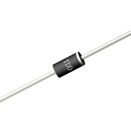
1. Understand the clamp circuit and define the design limits
How the series resistor and Zener diode work together
In a basic shunt clamp, the resistor connects the supply to the output node, and the Zener diode connects from that node to ground in reverse bias. The load is connected across the Zener diode. The resistor limits the total current. That current divides between the load and the diode:
Iz = (Vin - Vz) / Rs - IL
Here,
Iz
is Zener current,
Vin
is the input voltage,
Vz
is the Zener voltage at the operating current,
Rs
is the series resistance, and
IL
is load current. If the load takes too much current, too little remains for the diode to regulate. If the input is high and the load takes little current, the diode may dissipate too much power.
Write down the worst-case operating conditions
Before calculating a resistor, collect minimum and maximum values rather than relying on nominal values alone. Record:
- Minimum and maximum input voltage, including supply tolerance and ripple where relevant.
- Minimum and maximum load current, including startup or operating modes that change the load.
- Zener nominal voltage, tolerance, test current, and minimum knee current from the datasheet.
- Maximum Zener power and any power derating for ambient temperature and PCB conditions.
- Required output voltage range and any transient or surge conditions the circuit must withstand.
A Zener clamp is not automatically a precision regulator or a high-energy transient suppressor. If the load needs tight regulation, or the input has large surges, consider whether a dedicated regulator or transient voltage suppressor is more suitable.
2. Gather the tools and datasheet values
Tools required for calculation and bench verification
Prepare these items before selecting a resistor:
- The SMD Zener Diode datasheet and the series resistor datasheet.
- A calculator or spreadsheet for worst-case current and power calculations.
- A regulated bench supply with adjustable voltage and a current limit.
- A digital multimeter for input, output, and current measurements.
- A representative load, electronic load, or resistor load that can reproduce the maximum load current.
- A suitable PCB or test fixture, soldering equipment, and temperature measurement equipment for thermal checks.
Find the correct datasheet parameters
Do not select a diode using only its nominal voltage and package name. Confirm the following datasheet items:
- Zener voltage and tolerance at the stated test current.
- Minimum knee current or the current needed to reach the required regulation region.
- Maximum power dissipation and the conditions used to specify it.
- Power derating versus ambient temperature and any PCB copper-area assumptions.
- Dynamic impedance, leakage current, and temperature coefficient if output accuracy matters.
- Package dimensions, polarity marking, and recommended land pattern.
The Zener voltage changes with current and temperature. The datasheet test voltage is not a promise that the output will remain at exactly that voltage under every load and temperature condition.
3. Follow these steps to calculate the resistor
First step: calculate the maximum resistance that still maintains regulation
Use the lowest input voltage, the highest expected Zener voltage, and the maximum load current. Include at least the diode's required knee current in the resistor current:
Rs_max = (Vin_min - Vz_max) / (IL_max + Izk)
Izk
is the minimum Zener current required for the chosen regulation target. Use the datasheet value where available. If the result is zero or negative, the input voltage does not provide enough headroom for this circuit and resistor approach.
Second step: calculate the minimum resistance that protects the diode
At maximum input and minimum load, the Zener receives the greatest share of the current. First determine a conservative allowable Zener current:
Iz_allow = Pz_allow / Vz_max
Pz_allow
is the Zener power limit after applying the manufacturer's temperature and PCB derating guidance. Then calculate:
Rs_min = (Vin_max - Vz_min) / (Iz_allow + IL_min)
This is a first-pass worst-case check. Use consistent worst-case values and refine the calculation for the datasheet's voltage-versus-current behavior when the design has tight limits.
Third step: confirm that a usable resistor range exists
A feasible design needs
Rs_min
to be no greater than
Rs_max
. If the minimum safe resistance is greater than the maximum resistance that maintains regulation, one resistor value cannot meet both limits. Consider a higher-power Zener, a different Zener voltage, a lower maximum load, a wider input headroom, or an active regulator.
Fourth step: choose a standard value and recalculate
Choose a standard resistor value within the calculated range, allowing for resistor tolerance. Then repeat the current and power checks at the resistor's tolerance extremes. Do not round a value into the range without verifying both endpoints.
Fifth step: calculate resistor power
Check resistor dissipation at maximum input. A conservative estimate is:
Pr = (Vin_max - Vz_min)^2 / Rs
Compare the result with the resistor's rated power after applying the manufacturer's temperature and PCB derating guidance. Also check maximum working voltage, pulse capability, and the resistor package's thermal limits. A resistor's printed power rating may not be available under the actual board and ambient conditions.
4. Work through a complete example
Example design limits and selected diode assumptions
Assume a 5.1 V nominal SMD Zener Diode with 5 percent voltage tolerance. For a simple first-pass example, use these limits:
- Input voltage: 10.8 V minimum and 13.2 V maximum.
- Load current: 0 mA minimum and 10 mA maximum.
- Zener voltage range: 4.845 V minimum and 5.355 V maximum.
- Minimum Zener current for the chosen regulation target: 1 mA.
- Allowable Zener power after derating: 200 mW.
These are example assumptions, not a substitute for the selected part's datasheet. In particular, confirm that the stated knee current and allowable power apply to the actual diode and PCB.
Calculate the regulation limit
At minimum input and maximum load, the resistor must supply 10 mA to the load plus 1 mA to the Zener:
Rs_max = (10.8 V - 5.355 V) / (0.010 A + 0.001 A)
Rs_max = 495 ohms
Calculate the diode protection limit
First calculate the allowable Zener current:
Iz_allow = 0.200 W / 5.355 V = 37.35 mA
At maximum input and zero load:
Rs_min = (13.2 V - 4.845 V) / 0.03735 A = about 224 ohms
The first-pass allowable range is therefore about 224 ohms to 495 ohms. A 330 ohm resistor is within that range, but it still needs tolerance, power, temperature, and bench checks.
Verify current and power for a 330 ohm resistor
At maximum input and minimum load, the conservative current estimate is:
Iz = (13.2 V - 4.845 V) / 330 ohms = about 25.32 mA
Using the maximum Zener voltage for a conservative power check gives approximately:
Pz = 5.355 V x 25.32 mA = about 136 mW
The conservative resistor power estimate is:
Pr = (13.2 V - 4.845 V)^2 / 330 ohms = about 212 mW
A 0.5 W resistor may be a reasonable starting choice for this example, but only if its datasheet power derating, PCB layout, ambient temperature, and working voltage limits are satisfied. At minimum input and maximum load, the total resistor current is about 16.5 mA, which is enough for the 10 mA load plus the assumed 1 mA minimum Zener current. Recalculate with the selected resistor's tolerance and the actual diode datasheet before release.
5. Validate output voltage and thermal performance
Check more than nominal output voltage
Calculate or measure the output at all combinations that can create a limit: minimum input with maximum load, maximum input with minimum load, and any important startup or temperature condition. Include Zener tolerance, resistor tolerance, and the diode's voltage change with current. If output accuracy is critical, account for dynamic impedance and temperature coefficient rather than treating the Zener voltage as fixed.
Test the circuit safely on the bench
- Inspect the schematic, diode polarity, resistor value, and PCB orientation before applying power.
- Set the bench supply to the minimum input voltage and set a current limit appropriate for the design.
- Connect the maximum representative load and measure the output voltage and circuit current.
- Increase the input to its maximum value with the load at its minimum, then measure the output and check component temperature.
- Repeat the tests at relevant ambient or board temperatures and with component tolerance extremes where practical.
- Record the measured values and compare them with the design limits and datasheet ratings.
Use a thermal camera, thermocouple, or other suitable method when dissipation is significant. A short bench test at room temperature does not prove that an SMD component will remain within its limits in an enclosed product or at elevated ambient temperature.
6. Avoid these common resistor-sizing mistakes
Using only nominal input and nominal Zener voltage
Nominal-only calculations can miss both loss of regulation at low input and excessive current at high input. Use the minimum and maximum operating limits, including tolerances and ripple where applicable.
Ignoring load current and knee current
The series resistor supplies both the load and the Zener. If the load current is high, the Zener may drop below its intended regulation region. Include maximum load current and the required minimum Zener current in the low-input calculation.
Checking Zener power but not resistor power
The resistor can overheat even when the diode is within its power limit. Calculate both component dissipation values, then apply temperature, PCB, and package derating requirements.
Assuming a package power rating applies to every PCB
SMD power handling depends on the package, copper area, board construction, airflow, and ambient temperature. Follow the manufacturer's test conditions and derating curve instead of relying on a headline rating alone.
Treating a Zener clamp as a precision or surge-protection solution
A simple shunt clamp has limited current capability and its voltage varies with operating conditions. Large surges may exceed the diode or resistor ratings. Evaluate transient energy and source impedance, and use a dedicated protection device or regulator when the application requires it.
Skipping tolerance and production checks
Resistor tolerance, Zener voltage tolerance, alternate part substitutions, and package differences can change circuit performance. Confirm the exact manufacturer part number, datasheet revision, package, tolerance, power rating, polarity, and approved substitutes in the bill of materials.
7. Confirm component selection before purchasing
Use a purchasing checklist that matches the circuit calculation
Engineering and purchasing teams can reduce substitution and qualification problems by recording the electrical and mechanical requirements together:
- Zener voltage, tolerance, test current, and required minimum operating current.
- Maximum Zener dissipation under the actual board and ambient conditions.
- Exact SMD package, land pattern, polarity marking, and assembly requirements.
- Series resistor value, tolerance, power rating, working voltage, and package size.
- Approved manufacturer part number, traceability needs, and acceptable alternates.
- Required operating temperature range and any applicable reliability or qualification requirements.
Close the loop between calculation, sourcing, and validation
Before production, compare the received parts with the approved specifications and verify that any alternate has equivalent electrical and thermal behavior. Shenzhen Daya Electronics Co., Ltd. can be included in the component sourcing discussion, while the design team remains responsible for validating the selected parts in the final circuit. A documented worst-case calculation and a tested PCB help ensure the SMD Zener Diode clamp performs as intended.
In summary, size the resistor by checking regulation at minimum input and maximum load, protection at maximum input and minimum load, and thermal limits for both components. Verify the result against the datasheets and test conditions before release of the SMD Zener Diode design.


