A Solar Bypass Diode helps a photovoltaic module keep producing power when shade or a damaged cell limits current through part of the module. Choosing between Schottky and PN diodes affects forward voltage loss, junction-box temperature, reverse leakage, and long-term reliability. This guide compares the options and explains what buyers should verify before selecting a part.
Searchers comparing these diode types generally need more than a definition. They want understandable specifications, realistic thermal and field-performance considerations, guidance on battery-system effects, and a practical way to avoid selecting a diode that is undersized or poorly matched to the module. The sections below address those decision points.
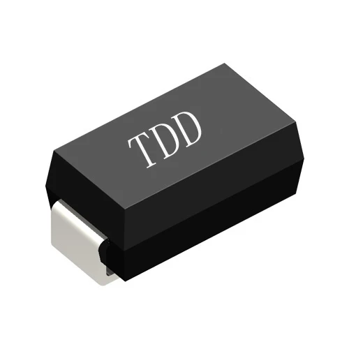
Shenzhen Daya Electronics Co., Ltd. works with electronic components used in solar applications. When evaluating a supplier or part, buyers should still confirm the exact datasheet, traceability, and suitability for their module design rather than relying on a product category alone.
Start with the protection job, not the diode label
Understand what a bypass diode does in a PV module
A bypass diode is connected across a cell substring, normally in reverse bias while the substring is operating normally. If shading or a fault forces that substring into reverse bias, the diode can conduct around it. This reduces the risk of damaging hot spots and helps the remaining module sections continue supplying current.
- A bypass diode protects a cell substring from excessive reverse-bias stress.
- It can reduce the power penalty caused by partial shading, but it does not make a shaded module operate at full output.
- It is not the same as a series blocking diode, which is used to limit reverse current between strings or from a battery.
- The number of diodes and their placement depend on module architecture and the manufacturer's design.
Recognize the purchasing questions behind the comparison
When buyers compare first-page articles and product information, the recurring questions are usually practical: which diode wastes less power, which one runs cooler, whether a lower forward voltage is always better, and whether the part will survive high module temperatures. Installers and procurement teams also need to confirm current and voltage margins, junction-box compatibility, documentation, and consistent supply.
The useful comparison is therefore not simply Schottky versus PN. It is the performance of a specific diode, in a particular package and junction-box layout, under the electrical and environmental conditions of the module.
Compare the electrical and thermal parameters that determine fit
Use typical ranges as screening values, not as a substitute for a datasheet
The figures below are broad examples of commonly encountered design tendencies. They are not guaranteed limits for every diode. The exact values depend on the part number, current, temperature, package, and test conditions listed by the manufacturer.
| Parameter | Schottky diode, typical tendency | PN silicon diode, typical tendency | What the buyer should check |
|---|
| Forward voltage drop | Often about 0.3 to 0.6 V at relevant operating currents | Often about 0.7 to 1.1 V at relevant operating currents | Read the forward-voltage curve at the actual bypass current and expected junction temperature. |
| Forward power loss | Often lower for the same current because of the lower forward drop | Often higher at the same current | Estimate loss as forward voltage multiplied by current, then assess how that heat leaves the junction box. |
| Reverse leakage | Often higher and more sensitive to temperature | Often lower at comparable conditions | Check leakage at the maximum expected operating temperature, not only at room temperature. |
| Reverse-voltage rating | Part-dependent; many solar designs use ratings selected for the substring and transient conditions | Part-dependent; some designs offer higher reverse-voltage options | Confirm the maximum reverse voltage, system configuration, and applicable design margin. |
| Current rating | Available across a wide range, including high-current packages used in modules | Available across a wide range | Compare the rating with module short-circuit current, expected bypass current, and relevant derating conditions. |
| Thermal capability | Depends strongly on die, package, mounting, and junction-box cooling | Also depends strongly on die, package, mounting, and junction-box cooling | Review maximum junction temperature, thermal resistance, lead or tab layout, and the assembled box temperature. |
| Cost and availability | Can be attractive where low forward loss is important; cost varies by specification and supply | May be economical and available in established packages; cost varies by specification and supply | Compare qualified part numbers, not just diode families or headline prices. |
Calculate loss and temperature for the actual operating point
A first-pass conduction-loss estimate is P = Vf x I, where Vf is the forward drop at the expected current and temperature, and I is the bypass current. For example, a lower Vf can reduce the heat generated while the diode conducts. However, that result does not by itself prove the diode will run cooler in the finished junction box: thermal resistance, copper area, encapsulation, ambient temperature, and neighboring components also matter.
- Use the datasheet forward-voltage curve rather than a single headline value.
- Check the diode's current rating under the specified mounting and temperature conditions.
- Calculate or measure the junction temperature using the package thermal data and the actual enclosure design.
- Allow suitable margin for high ambient temperature, manufacturing variation, and the module's intended service conditions.
Weigh the real advantages and disadvantages of each diode type
Schottky diodes favor lower conduction loss
A Schottky diode is often selected for solar bypass service because its lower forward voltage can reduce power dissipation when bypass current flows. This can be valuable in a compact junction box where heat is difficult to remove. Its strengths do not remove the need to check reverse leakage, voltage rating, and hot operating behavior.
- Advantages: generally lower forward drop, lower conduction loss at a comparable current, and broad availability in power packages.
- Disadvantages: reverse leakage can rise substantially with temperature, reverse-voltage capability varies by part, and thermal performance still depends on the complete assembly.
- Often worth evaluating when reducing bypass-mode loss and junction-box heat is a priority and the selected part meets reverse-voltage and temperature requirements.
PN diodes can suit designs that prioritize leakage and voltage margin
A PN silicon diode generally has a higher forward drop than a comparable Schottky diode, which can mean more heat during bypass conduction. Depending on the specific part, it may offer lower reverse leakage or a useful reverse-voltage rating. These are tendencies, not a guarantee that every PN diode will outperform every Schottky diode in a given module.
- Advantages: some parts provide lower reverse leakage and useful reverse-voltage options, and the technology is widely established.
- Disadvantages: the higher forward drop can increase bypass-mode power loss and heat, especially at substantial current.
- Often worth evaluating when the specific part's leakage, voltage rating, qualification, and supply characteristics fit the design better than the available Schottky alternatives.
In either category, a diode that exceeds its thermal or electrical limits is not a reliable choice. A well-qualified PN diode can be preferable to an unsuitable Schottky part, and a properly rated Schottky diode can be preferable where conduction loss is the key constraint.
Set realistic expectations for field performance and battery impact
Relate bypass behavior to energy yield, not a promise of longer battery life
A bypass diode does not directly extend a battery's chemical service life. Its effect on a battery-based system is indirect: during partial shading, a functioning bypass path may let the unshaded portions of a module continue contributing power. Depending on shading patterns, system controls, and the battery's charge state, that can improve available charging energy compared with a failed or missing bypass path.
There is no universal battery-life improvement percentage for switching from a PN diode to a Schottky diode. The energy difference depends on how often the diode conducts, the current during those periods, the forward-voltage difference between the chosen parts, module layout, local shading, and charge-controller behavior. Under normal unshaded operation, a bypass diode is typically reverse-biased, so its forward-drop advantage does not translate into continuous energy gain.
Evaluate stability with operating data and inspection
In service, the most useful comparison is whether the selected diode stays within its temperature and electrical limits over real operating cycles. A lower forward loss may help reduce heat during bypass events, while elevated reverse leakage in a hot Schottky device deserves attention during design verification. Neither diode family alone guarantees long service life.
- Record module and junction-box temperatures during hot, high-irradiance operation.
- Observe output during repeatable partial-shading conditions and compare it with an unshaded baseline.
- Check for abnormal heating, discoloration, cracking, loose connections, or water ingress during scheduled inspection.
- For product qualification, test representative assemblies through the manufacturer's required electrical, thermal, environmental, and reliability procedures.
These checks distinguish diode behavior from other causes of poor yield, such as dirty modules, poor connections, incompatible module strings, or charge-controller configuration.
Choose a diode using a repeatable selection process
Verify ratings, package, and application conditions before ordering
Procurement teams can reduce substitution risk by documenting the application and reviewing the complete datasheet for each proposed part. Do not approve a replacement solely because the package looks similar or the maximum current number appears adequate.
- Confirm whether the component is a bypass diode and identify the substring it protects.
- Determine the module's maximum relevant current and reverse-voltage conditions, including design margins and applicable transient considerations.
- Compare forward voltage at the expected current and temperature, then estimate power dissipation during bypass operation.
- Check reverse leakage over the intended temperature range and confirm the maximum junction temperature.
- Verify package dimensions, terminal arrangement, mounting method, insulation, and compatibility with the junction-box layout.
- Review qualification documents, traceability, production consistency, and the supplier's change-control process.
- Validate the selected part in a representative module or junction-box assembly before volume deployment.
Match the recommendation to the purchasing group
- Module designers: compare both diode types using real current, thermal, and enclosure data, then validate the complete assembly.
- Installers and system integrators: use the module maker's approved replacement specification and avoid mixing unverified parts in a string.
- Procurement teams: compare exact part numbers, documentation, lot traceability, and stable supply in addition to price.
- Small system owners: do not replace a junction-box diode without confirming module compatibility and safe service procedures with a qualified professional.
Make the final choice from the system trade-off
Use a short decision checklist before approval
For many modern module designs, a Schottky diode is the leading candidate when lower forward loss is important and its hot reverse-leakage behavior, reverse-voltage rating, and thermal design are acceptable. A PN diode can be a sound choice when its particular leakage, voltage, qualification, or sourcing profile better matches the application and its additional forward loss can be managed.
- Choose the exact diode from verified ratings and test conditions, not from technology name alone.
- Prioritize thermal design because both diode types can fail when current, ambient temperature, or heat removal exceeds their limits.
- Assess battery-system benefits as possible energy-yield differences under shading, not as a direct battery-life guarantee.
- Require traceable parts and module-level validation for safety-critical or high-volume purchasing.
Ultimately, the best Solar Bypass Diode is the part that protects the intended substring, meets its electrical and thermal limits with margin, and remains consistently available with reliable documentation. Shenzhen Daya Electronics Co., Ltd. can be considered as part of a sourcing evaluation, while final approval should always rest on the exact datasheet and validation results for the module design.


